Custom Optical Coatings
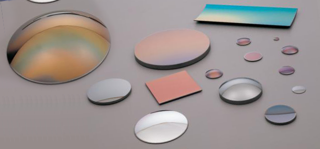
Leveraging a broad technology portfolio and decades of experience, VIAVI OSP can design and manufacture virtually any interference filter that obeys the laws of physics. Use the links below to explore our capabilities, or contact us to learn more.

Low Angle Shift
All interference filters shift to shorter wavelengths with increasing angle of incidence. This can be an advantage, as in color-shifting pigments, but often presents an unwelcome challenge to optical system designers working in fixed wave bands. The VIAVI OSP LAS (low angle shift) technology combines proprietary design, materials, and processes that dramatically reduce angle shift and offer the system designer unprecedented control over performance variation and signal-to-noise ratio, especially in 3D depth sensing camera systems. Contact us to learn more.

Large and Meter Class Optics
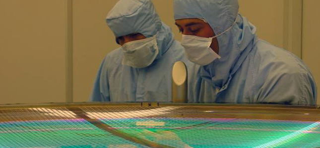
With roots in specialty, large scale optics, VIAVI OSP remains capable of high-precision, environmentally-robust coatings on optics up to 2.5 meters. Our reconfigurable, large optics chamber is adjacent to a dedicated ISO Class 5 clean room and equipped with large-optics handling facilities and custom tooling capability.

Visible and NIR Coatings
VIAVI OSP produces visible and NIR filters with high transmission, deep blocking, and sharp, precise, and repeatable edges.
MWIR Coatings
VIAVI OSP produces mid-wave infrared (MWIR) filters with high transmission, deep blocking, and sharp, precise, repeatable edges.
LWIR Coatings
VIAVI OSP produces longwave infrared (LWIR) filters with high transmission, deep blocking, and sharp, precise, repeatable edges. We specialize in patterned antireflection coatings for microbolometer lid wafers.
Polarization Control
Myriad devices, including displays, magnetometers, and 3D depth sensing cameras, depend on precision control of polarization state for peak performance. Our custom waveplates – tilted c-plates, a-plates, and hybrid components – are built from a unique combination of organic and inorganic materials using advanced wafer-level processes.